 注: 建议图片大小150px*50px

丨
English
注: 建议图片大小150px*50px Views: 0 Author: Site Editor Publish Time: 2026-10-14 Origin: Site


Microchips drive our modern world today. They power everything from electric vehicles to complex artificial intelligence data centers. However, manufacturing these silicon lifelines requires absolute perfection. Looking at current industry trends, the rapid expansion of generative AI and high-speed telecommunication networks is pushing semiconductor fabrication nodes down to 3 nanometers and below. This relentless miniaturization means equipment manufacturers face unprecedented pressure. They must localize their supply chains to mitigate global disruptions. Simultaneously, they demand exponentially tighter tolerances from their vendors. Even a microscopic error or a single stray particle can ruin an entire batch of expensive wafers. In this unforgiving landscape, Precision Machining emerges as the definitive solution. It solves these complex engineering demands by providing the exact mechanical properties and structural integrity required for modern chip fabrication.
Unmatched Accuracy: CNC machining delivers the sub-micron tolerances and high repeatability strictly required for wafer processing equipment.
Material Versatility: Advanced materials, including specialized aluminum alloys, stainless steel, and high-performance plastics, are efficiently processed using multi-axis technology.
Integrated Fabrication: Beyond machined components, custom sheet metal and heavy-duty welded frames play a crucial role in housing and stabilizing delicate machinery.
Vendor Selection: Choosing the right manufacturing partner requires evaluating their cleanroom compliance, stringent quality control standards, and full-stack fabrication capabilities.
The semiconductor sector operates on the absolute cutting edge of physics and material science. Driven by the relentless push for smaller, faster, and more power-efficient microchips, manufacturers are now developing transistors at single-digit nanometer scales. At these microscopic dimensions, the margin for error within the manufacturing environment effectively drops to zero. Equipment used in lithography, etching, and deposition must function with absolute stability. Even the slightest thermal expansion or mechanical vibration can derail the entire production process.
Recent industry shifts toward extreme ultraviolet lithography and advanced 3D packaging have fundamentally changed equipment design rules. Engineers are no longer just dealing with microscopic scales. They are managing atomic-level material deposition. This requires structural frames and vacuum chambers that exhibit zero thermal drift during high-power plasma cycles.
Furthermore, one of the most critical challenges is the industry's zero-tolerance policy for contamination. Engineers working in Class 100 or Class 10 cleanrooms know the risks intimately. A microscopic speck of dust, a stray metal particulate, or slight chemical outgassing from a machine component can compromise a million-dollar silicon wafer batch. Consequently, equipment parts must exhibit flawless surface finishes and undergo rigorous cleaning protocols before ever entering the fabrication facility.
These components frequently operate in extreme physical conditions. Semiconductor fabrication involves ultra-high vacuum environments, extreme temperature fluctuations, and continuous exposure to highly corrosive plasma and reactive gases. Standard manufacturing methods simply cannot produce parts capable of withstanding these stresses while maintaining dimensional stability over thousands of operational hours.
Navigating the strict parameters of semiconductor fabrication is incredibly challenging. Equipment manufacturers require a production method offering unparalleled control and predictability. Advanced CNC technology stands out as the primary solution here. It provides specific technical benefits that align directly with rigorous industry standards.
Semiconductor equipment consists of complex assemblies where multiple intricate parts must fit together flawlessly. A misalignment of a fraction of a millimeter can compromise a vacuum seal or disrupt a delicate laser path. On the shop floor, achieving a true position tolerance of ±0.001 millimeters on a 5-axis machining center requires more than just good equipment. It demands strict thermal compensation and rigid workholding. This level of sub-micron accuracy ensures that critical components, such as kinematic mounts and optical alignment frames, perform their designated functions without introducing mechanical deviations. Advanced thermal compensation software and rigid machine tooling further ensure that dimensional accuracy remains consistent, even as cutting friction generates heat throughout the machining cycle.
Achieving high accuracy on a single prototype is impressive. However, semiconductor equipment manufacturers require that exact same accuracy across hundreds or thousands of parts. Automated CNC systems excel in providing this exceptional repeatability. Through rigorous statistical process control and automated tool wear monitoring, the machining process guarantees that the thousandth part produced is statistically identical to the first. This repeatability is a critical requirement for scaling fleet equipment production. It ensures that replacement parts offer predictable, standardized performance without requiring custom recalibration on the cleanroom floor.
Modern semiconductor parts are rarely simple geometric shapes. They often feature intricate internal channels, undercut features, and complex surface profiles. These are absolutely necessary for advanced cooling systems, precise gas distribution, or robotic wafer handling. Such complex geometries cannot be cast or molded with the required precision. Simultaneous 5-axis milling allows cutting tools to approach the workpiece from virtually any angle. This enables the creation of fluid dynamics channels and lightweight structural lattices directly from solid blocks of high-purity material.
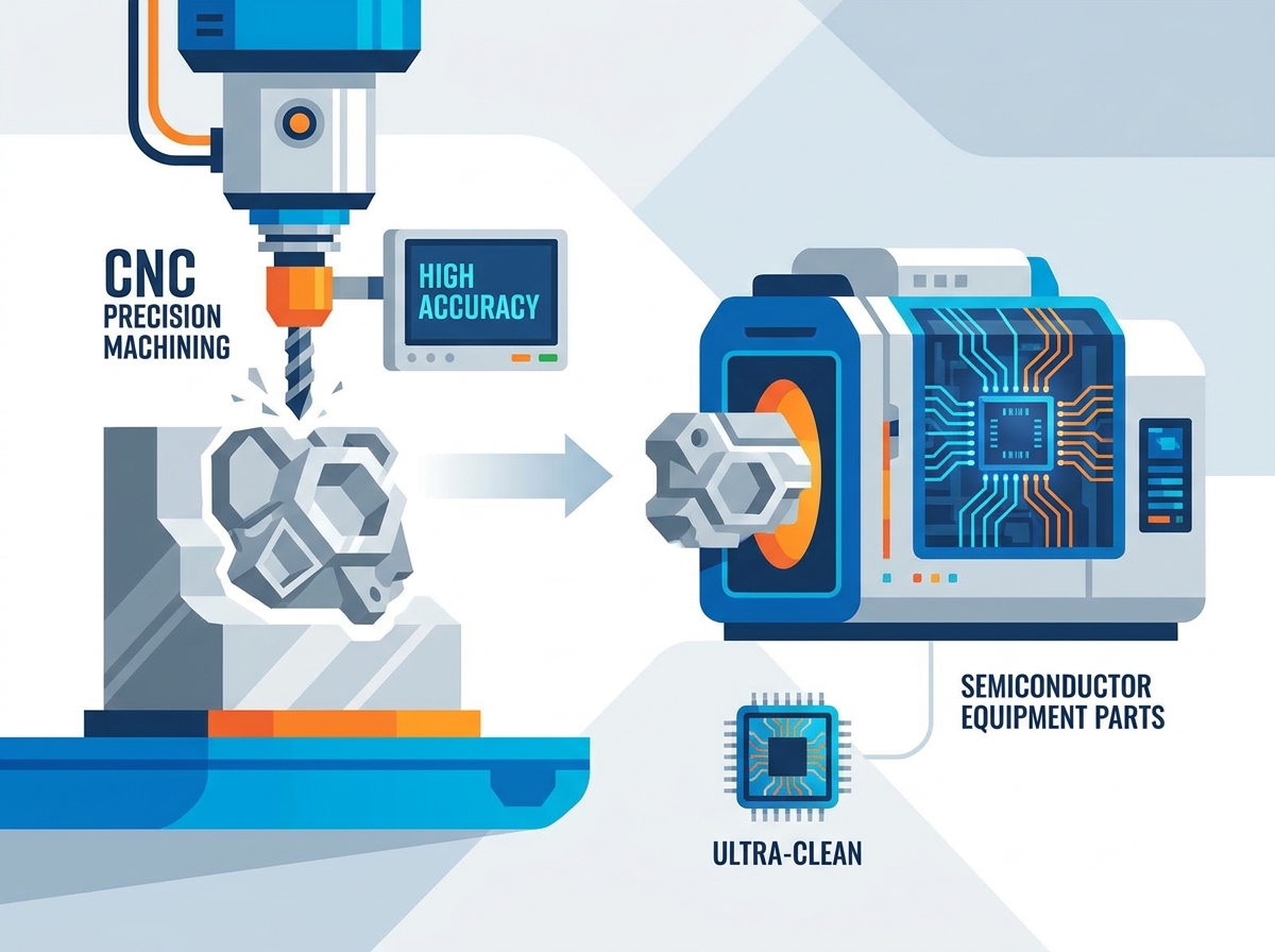
The theoretical benefits of advanced machining translate directly into the high-performance components that make up the anatomy of a semiconductor fabrication plant. These parts execute highly specific tasks where failure is simply not an option.
Silicon wafers are incredibly fragile. They are highly susceptible to mechanical damage and surface contamination. When a robotic end-effector transfers a 300-millimeter wafer, any vibration or surface imperfection can cause microscopic scratches. Vacuum chucks, which hold the wafer securely during processing, require perfectly flat and smooth surfaces to prevent localized stress. Similarly, wafer carriers are meticulously milled to provide rigid, vibration-free support while minimizing physical contact with the delicate wafer edges.
Chemical vapor deposition and etching processes rely on the highly controlled delivery of reactive gases. Components like showerheads, gas manifolds, and valve housings are manufactured using specialized micro-machining techniques. These parts demand flawless internal finishes. Engineers often measure these in extremely low surface roughness values to prevent gas turbulence, particle entrapment, or uneven chemical distribution. Any internal burrs left behind during manufacturing could lead to catastrophic gas contamination.
Many semiconductor processes occur in ultra-high vacuum chambers to prevent atmospheric interference. The structural elements making up these chambers must maintain absolute integrity under extreme pressure differentials. These include massive aluminum lids, sealing flanges, and active cooling plates. Precise tool paths ensure that O-ring grooves and metal-to-metal sealing surfaces are cut with exacting precision. This guarantees a completely leak-proof environment even when subjected to rapid thermal cycling.
While micro-machined internal valves handle delicate fluid dynamics, the overall stability and safety of a photolithography or etching machine rely heavily on its outer architecture. A comprehensive manufacturing approach seamlessly integrates these secondary structural elements to form a complete, robust tool.
| Fabrication Process | Primary Semiconductor Application | Standard Precision Level | Key Engineering Value |
|---|---|---|---|
| CNC Precision Machining | Vacuum chambers, gas showerheads, wafer chucks | Down to ±0.001 millimeters | Provides absolute dimensional stability and flawless sealing surfaces. |
| Custom Sheet Metal | Control cabinets, machine guarding, cleanroom enclosures | ±0.1 millimeters | Ensures electromagnetic shielding and precise airflow management. |
| Heavy-Duty Welding | Vibration-dampening base frames, structural chassis | Post-weld milling required for flatness | Delivers massive rigidity to prevent optical misalignment. |
Semiconductor machinery requires robust protection from the external environment. It also needs shielding to protect operators from high-voltage electronics and laser systems. Specifically, custom Sheet Metal Parts are utilized to construct the protective outer chassis, electrical control cabinets, and machine guarding. The fabrication of these parts demands precise laser cutting and CNC press brake bending to ensure seamless panel alignment. High-quality sheet metal integration ensures that enclosures are not only aesthetically clean but also structurally sound. They provide necessary electromagnetic interference shielding and strict airflow management for cleanroom compatibility.
The foundation of any semiconductor tool must be exceptionally rigid. Microscopic vibrations from facility floors or internal motors can easily misalign optics or disrupt wafer positioning. To counteract this, heavy-duty Welded Structural Components provide a massive, vibration-dampening framework necessary to support delicate internal assemblies. Fabricating these frames requires precision welding techniques, followed by rigorous thermal stress-relieving processes in large industrial ovens. Once welded and stress-relieved, critical mounting points on the frame often undergo secondary milling. This ensures the final assembly surfaces are perfectly flat and parallel.
The extreme environments inside semiconductor equipment dictate strict material selection. Raw materials must exhibit specific thermal properties, resist corrosive chemicals, and maintain exceptionally low outgassing rates under deep vacuum.
Aluminum is highly favored in semiconductor manufacturing due to its excellent machinability, high strength-to-weight ratio, and superior thermal conductivity. Alloys like 6061 and 7075 are frequently used for structural components, robotic arms, and vacuum chamber bodies. Aluminum is particularly valuable because it can be easily anodized. This creates a hard, non-reactive surface layer that prevents particulate shedding and resists mild chemical exposure.
When equipment parts are exposed to highly corrosive etching gases or require exceptional mechanical strength, stainless steel becomes the material of choice. Grades like 316L offer outstanding resistance to localized corrosion and pitting. Engineers commonly specify this material for gas lines, high-pressure flanges, and fluid control manifolds. While stainless steel is inherently more challenging to cut than aluminum, rigid setups and specialized carbide tooling allow seasoned machinists to achieve the necessary tight tolerances.
Not all semiconductor components can be metallic. Parts requiring electrical insulation, extreme chemical inertness, or high-temperature resistance are machined from advanced engineering plastics and ceramics. Materials like Polyetheretherketone and Polytetrafluoroethylene are frequently used for insulators, seals, and wafer guides. Managing the heat buildup when milling these plastics requires specialized coolant strategies to prevent the material from warping or melting. Additionally, Quartz and advanced ceramics are ground and machined for their high thermal stability and absolute purity.
In the semiconductor sector, the manufacturing process does not end when the spindle stops turning. Post-machining treatments are strictly mandatory. They ensure parts do not introduce deadly contaminants into the fabrication facility.
Machined surfaces, even those that appear perfectly smooth to the naked eye, can harbor microscopic burrs or reactive metal ions. Specialized surface treatments are applied to mitigate these risks. Electropolishing is widely used on stainless steel parts to dissolve microscopic surface peaks. This results in an ultra-smooth, passive surface that resists corrosion and prevents particle entrapment. For aluminum components, hard anodizing and specialized passivation processes create a dense oxide layer that permanently seals the metal.
Outgassing is the release of trapped gases or volatile organic compounds from a material in a vacuum. It is a critical threat to semiconductor yield. To prevent this, machined parts undergo rigorous, multi-stage ultrasonic cleaning using highly purified solvents and deionized water. Following cleaning, parts are often subjected to vacuum baking to force the outgassing of any remaining volatiles. Finally, components are packaged in certified cleanrooms using specialized anti-static, low-outgassing bagging materials.
Procuring components for semiconductor manufacturing equipment is fundamentally an exercise in risk management. The financial consequences of component failure, contamination, or micro-level dimensional inaccuracies are severe. Therefore, evaluating a manufacturing partner requires looking far beyond basic milling capabilities. Decision-makers must conduct rigorous audits of a supplier’s technological infrastructure, quality management systems, and overall fabrication ecosystem.
The foundation of semiconductor component manufacturing lies in the caliber of the machinery utilized. Standard 3-axis milling centers are generally insufficient for the complex geometries required by modern wafer processing equipment. An ideal manufacturing partner must possess state-of-the-art 5-axis machining centers. These machines allow for the continuous milling of complex internal channels, angled ports, and multi-faceted vacuum chamber components without the need to manually reposition the workpiece. This directly minimizes tolerance stack-up errors.
Technical expertise must also extend to the environmental control of the facility itself. Sub-micron cutting is highly susceptible to thermal expansion. Leading suppliers maintain strictly climate-controlled shop floors where temperature fluctuations are kept to an absolute minimum. This ensures that the thermal drift of both the machine tool and the raw material does not compromise dimensional accuracy.
In this industry, quality control cannot be an afterthought. It must be an integrated, data-driven process. The baseline requirement for any supplier is an active ISO 9001 certification, but true capability is proven through their metrology department. Suppliers must utilize advanced Coordinate Measuring Machines equipped with highly sensitive touch probes and optical scanning capabilities to verify complex geometries against original computer-aided design models.
Material traceability is equally critical. A reliable partner will provide comprehensive documentation, including Material Test Reports and Certificates of Conformance. This ensures that no counterfeit or low-grade alloys enter the supply chain. Full lot traceability and elemental analysis are non-negotiable standards for fab-ready components.
Relying on multiple fragmented suppliers for different components introduces logistical vulnerabilities, increases lead times, and complicates quality assurance. The most effective manufacturing partners operate as comprehensive solutions providers. Consolidating processes under one roof ensures uniform quality standards across the entire machine build. By partnering with a vendor capable of executing industry-leading CNC Precision Machining alongside advanced sheet metal fabrication and structural welding, semiconductor equipment companies can ensure stricter quality oversight and significantly reduce time-to-market.
Semiconductor components demand highly restrictive geometric dimensioning and tolerancing. Depending on the application, tolerances generally range from ±0.005 millimeters down to ±0.001 millimeters. For example, vacuum chamber sealing surfaces and ultra-high purity gas distribution manifolds require extreme flatness and sub-micron dimensional accuracy to prevent microscopic leaks. Achieving these tolerances requires rigid machine setups, specialized tooling, and strict thermal control of the machining environment.
Welded structural elements serve as the foundational architecture for manufacturing machinery. Tools such as photolithography machines and wafer inspection systems contain highly sensitive optics and micro-mechanisms that are easily disrupted by ambient facility vibrations. Heavy-duty, precision-welded frames provide the necessary rigidity and vibration-dampening characteristics. These frames undergo specialized thermal stress-relieving processes after welding to ensure they do not warp or distort over time.
Contamination control is a multi-step process that begins during machining and ends at final packaging. Manufacturers utilize specialized, low-residue cutting fluids and coolants that do not impregnate the material surface. After machining, components undergo mechanical deburring and multi-stage ultrasonic cleaning using specific chemical baths and deionized water. Finally, parts are subjected to specialized surface finishes, such as electropolishing or passivation, and are vacuum-sealed inside certified cleanrooms.
Thermal expansion is a critical variable in sub-micron manufacturing. As cutting tools engage with raw materials, friction generates heat, causing both the tool and the workpiece to expand microscopically. If unmanaged, a part machined to correct dimensions while warm will shrink out of tolerance as it cools. Elite manufacturers mitigate this by utilizing flood coolant systems, temperature-controlled shop environments, and advanced software that automatically compensates for thermal drift during the cutting cycle.
Extreme ultraviolet lithography operates in deep vacuum environments and utilizes highly complex mirror systems to direct light. CNC machining supports this transition by producing ultra-stable optical mounts, massive vacuum chamber housings, and highly efficient liquid cooling channels. These components must be machined from specialized low-expansion alloys to ensure the optical path remains perfectly aligned despite the massive heat generated by the plasma source.
Lead times vary significantly based on component complexity, material availability, and post-processing requirements. Simple structural brackets might take two to three weeks. In contrast, complex vacuum chambers requiring 5-axis milling, thermal stress relief, electropolishing, and cleanroom packaging can take eight to twelve weeks. Working with an integrated manufacturer who handles machining, welding, and sheet metal in-house drastically reduces these timelines by eliminating shipping delays between different subcontractors.
The modern semiconductor industry simply cannot exist without the microscopic accuracy provided by advanced manufacturing technologies. As chip architectures become increasingly complex and miniaturized, the equipment used to fabricate them must meet unprecedented standards of precision, material purity, and structural stability. From intricate internal gas manifolds to robust outer chassis frames, every single component plays a vital role in ensuring high wafer yields and operational safety.
Ultimately, selecting a highly capable manufacturing partner is one of the most critical strategic decisions an equipment builder can make. If your engineering team is struggling with thermal drift, vacuum leaks, or particulate contamination in your current machine builds, upgrading your component sourcing is the critical next step. We encourage you to review the full suite of semiconductor-grade manufacturing solutions at DN CNC Sheet Metal. By matching your specific operational requirements with our advanced machining, custom sheet metal, and heavy-duty structural framing capabilities, you can confidently build the next generation of total-reliability semiconductor machinery.


